
OPERATION MANUAL
The PCI bus multi-8255/8254 adapter provides total 24 digital I/O ports, each I/O port contains 8 I/O lines, and can be set either input or output by the user's program. Two 8254 on board chips provides six programmable interval timer/counter.
| 1. |
Turn off all power to your computer
and all peripheral devices before installing your multi-8255/8254 adapter. |
| 2. |
Remove the cover of the computer. |
| 3. |
Insert the multi-8255/8254 adapter
into any available PCI slot. Make sure the adapter is firmly seated in the
chosen slot. |
| 4. |
Replace the cover of the computer. |
| 5. |
Connects the expansion cables. |
| 6. |
Turn on the power of your computer, the PnP features will recognize the multi-8255/8254 adapter. |
Base + 1 : Port 1B input/output buffer.
Base + 2 : Port 1C input/output buffer.
Base + 3 : Port 1 control register.
Base + 4 : Port 2A input/output buffer.
Base + 5 : Port 2B input/output buffer.
Base + 6 : Port 2C input/output buffer.
Base + 7 : Port 2 control register.
Base + 8 : Port 3A input/output buffer.
Base + 9 : Port 3B input/output buffer.
Base + 10 : Port 3C input/output buffer.
Base + 11 : Port 3 control register.
Base + 12 : Port 4A input/output buffer.
Base + 13 : Port 4B input/output buffer.
Base + 14 : Port 4C input/output buffer.
Base + 15 : Port 4 control register.
Base + 16 : Port 5A input/output buffer.
Base + 17 : Port 5B input/output buffer.
Base + 18 : Port 5C input/output buffer.
Base + 19 : Port 5 control register.
Base + 20 : Port 6A input/output buffer.
Base + 21 : Port 6B input/output buffer.
Base + 22 : Port 6C input/output buffer.
Base + 23 : Port 6 control register.
Base + 24 : Port 7A input/output buffer.
Base + 25 : Port 7B input/output buffer.
Base + 26 : Port 7C input/output buffer.
Base + 27 : Port 7 control register.
Base + 28 : Port 8A input/output buffer.
Base + 29 : Port 8B input/output buffer.
Base + 30 : Port 8C input/output buffer.
Base + 31 : Port 8 control register.
Base + 32 : Counter 0 input/output buffer.
Base + 33 : Counter 1 input/output buffer.
Base + 34 : Counter 2 input/output buffer.
Base + 35 : Counter control register for counter 0,1,2.
Base + 36 : Counter 3 input/output buffer.
Base + 37 : Counter 4 input/output buffer.
Base + 38 : Counter 5 input/output buffer.
Base + 39 : Counter control register for counter 3,4,5.
 .
.
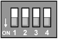
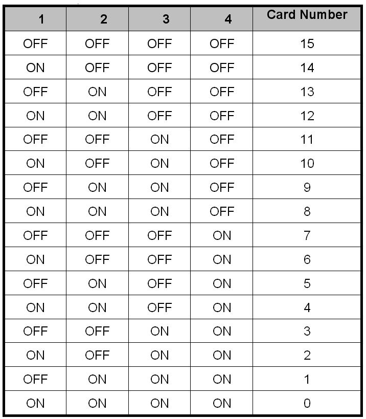
The card number starts from 0 to 15.
| Pin Assignments |
||||||||||||||||||||||||||||||||||||||||||||||||||||||||||||||||||||||||||||||||||||||||||||||||||||||||
| The signals are assigned in the DB40
and DB50 connector, its pin assignments are show in the below. |
||||||||||||||||||||||||||||||||||||||||||||||||||||||||||||||||||||||||||||||||||||||||||||||||||||||||
| 1. DB50 Connector Pin Assignments (CN1) | ||||||||||||||||||||||||||||||||||||||||||||||||||||||||||||||||||||||||||||||||||||||||||||||||||||||||
|
||||||||||||||||||||||||||||||||||||||||||||||||||||||||||||||||||||||||||||||||||||||||||||||||||||||||
| 1. DB50 Connector Pin Assignments (CN2) | ||||||||||||||||||||||||||||||||||||||||||||||||||||||||||||||||||||||||||||||||||||||||||||||||||||||||
|
||||||||||||||||||||||||||||||||||||||||||||||||||||||||||||||||||||||||||||||||||||||||||||||||||||||||
| 1. DB50 Connector Pin Assignments (CN3) | ||||||||||||||||||||||||||||||||||||||||||||||||||||||||||||||||||||||||||||||||||||||||||||||||||||||||
|
||||||||||||||||||||||||||||||||||||||||||||||||||||||||||||||||||||||||||||||||||||||||||||||||||||||||
| 1. DB50 Connector Pin Assignments (CN4) | ||||||||||||||||||||||||||||||||||||||||||||||||||||||||||||||||||||||||||||||||||||||||||||||||||||||||
|
||||||||||||||||||||||||||||||||||||||||||||||||||||||||||||||||||||||||||||||||||||||||||||||||||||||||
| 1. DB40 Connector Pin Assignments (CN5) | ||||||||||||||||||||||||||||||||||||||||||||||||||||||||||||||||||||||||||||||||||||||||||||||||||||||||
|