
INTRODUCTION
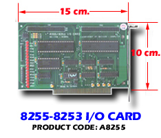
The 8255 I/O card is a programmable peripheral interface for PC/XT, PC/AT, 80386, 80486 or compatible. The interface card contains 8253 chips and 8255 chips, the 8253 chip provides programmable interval timer/counter functions and the 8255 chips provide programmable input/output functions.
The features of the 8255 I/O card are:
*Programmable I/O control functions.
*Up to 48 I/O lines.
*Maximum of 2MHZ count rate.
*Three independent 16 bits counter.
*Support several operating modes, which are Programmable.
*Sixteen LED indicate when I/O is operating.
*Port address
selectable.
PACKAGE CONTENTS:
*8255/8253 I/O card.
*8255/8253 user's manual.
*8255/8253terminator board (option).
*Two expansion flat cables (option).
HARDWARE CONFIGURATION
1.1 Configuration for DIP Switch
Before you use the 8255 I/O card, you must ensure that the I/O address and the clock are set correctly. Observe the figure below the proper settings for the 8255 I/O card are described in the following:
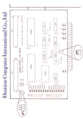
| 1. I/O
address JP2: Short (default) |
 |
Select &H300 -
&H30F as I/O port address. The I/O address correspond to three 8
bits ports and three counters are:
&H300: Port 1A
input/output buffer.
&H301: Port 1B input/output buffer.
&H302: Port 1C input/output buffer.
&H303: Port 1 control register.
&H304: Port 2A input/output buffer.
&H305: Port 2B input/output buffer.
&H306: Port 2C input/output buffer.
&H307: Port 2 control register.
&H308: Counter 0 input/output buffer.
&H309: Counter 1 input/output buffer.
&H30A: Counter 2 input/output buffer.
&H30B: Counter control register.
| I/O
address JP2: Open |
 |
&H360: Port 1A input/output buffer.
&H361: Port 1B input/output buffer.
&H362: Port 1C input/output buffer.
&H363: Port 1 control register.
&H364: Port 2A input/output buffer.
&H365: Port 2B input/output buffer.
&H366: Port 2C input/output buffer.
&H367: Port 2 control register.
&H368: Counter 0 input/output buffer.
&H369: Counter 1 input/output buffer.
&H36A: Counter 2 input/output buffer.
&H36B: Counter control register.
| 2. Clock
Selection |
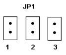 |
Select internal clock to counter 0.
JP1-2 = Short (default):
Select internal clock to counter 1.
JP1-3 = Short (default):
Select internal clock to counter 2.
JP1-1 = Open:
Select external clock to counter 0.
JP1-2 = Open:
Select external clock to counter 1.
JP1-3 = Open:
Select external
clock to counter 2.
2.2 Hardware Installation
Your 8255 I/O card is design to be inserted in any available slot in your PC/XT or compatibles. In order to gain access to the expansion slots and the program switches on the main board, follow the steps listed below:
1.Set the 8255 I/O card switch.
2.Turn off all power of your computer and all peripheral devices before installing your 8255 I/O card.
3.Remove the cover of the computer.
4.Insert your pre-configured card into any available slot. Make sure your I/O card is firmly seated in the chosen slot.
5.Replace the cover of the computer.
6.You are now ready
to use your 8255 I/O card for several Applications.
2.3 Pin
Assignment
|
PIN
|
1
|
GND
|
PIN
|
2
|
GND
|
| |
3
|
GND
|
|
4
|
PA3
|
| |
5
|
PA1
|
|
6
|
PA2
|
| |
7
|
CLK0
|
|
8
|
PA0
|
| |
9 |
GATE0
|
|
10
|
OUT0
|
| |
11
|
OUT2
|
|
12
|
CLK2
|
| |
13
|
CLK1
|
|
14
|
GATE2
|
| |
15
|
OUT1
|
|
16
|
GATE1
|
| |
17
|
PA5
|
|
18
|
PA4
|
| |
19
|
PA7
|
|
20
|
PA6
|
| |
21
|
PC6
|
|
22
|
PC7
|
| |
23
|
PC4
|
|
24
|
PC5
|
| |
25
|
PC1
|
|
26
|
PC0
|
| |
27
|
PB7
|
|
28
|
PC2
|
| |
29
|
PB6
|
|
30
|
PC3
|
| |
31
|
PB5
|
|
32
|
PB0
|
| |
33
|
PB4
|
|
34
|
PB1
|
| |
35
|
PB3
|
|
36
|
PB2
|
| |
37
|
+5V
|
|
38
|
-5V
|
| |
39 |
+12V
|
|
40
|
-12V
|
|
PIN
|
1
|
GND
|
PIN
|
2
|
GND
|
| |
3
|
GND
|
|
4
|
GND
|
| |
5
|
GND
|
|
6
|
GND
|
| |
7
|
GND
|
|
8
|
GND
|
| |
9 |
GND
|
|
10
|
GND
|
| |
11
|
GND
|
|
12
|
GND
|
| |
13
|
PA0
|
|
14
|
PA1
|
| |
15
|
PA2
|
|
16
|
PA3
|
| |
17
|
PA4
|
|
18
|
PA5
|
| |
19
|
PA6
|
|
20
|
PA7
|
| |
21
|
PC7
|
|
22
|
PC6
|
| |
23
|
PC5
|
|
24
|
PC4
|
| |
25
|
PC0
|
|
26
|
PC1
|
| |
27
|
PC2
|
|
28
|
PB7
|
| |
29
|
PC3
|
|
30
|
PB6
|
| |
31
|
PB0
|
|
32
|
PB5
|
| |
33
|
PB1
|
|
34
|
PB4
|
| |
35
|
PB2
|
|
36
|
PB3
|
| |
37
|
+5V
|
|
38
|
-5V
|
| |
39 |
+12V
|
|
40
|
-12V
|
DIAGNOSTIC
The diagnostic program is list in the following:
1. BASIC version
100 REM 8255 I/O CARD TESTI
101 NG PROGRAM
110 SCREEN 0,0,0: WIDTH 80,25: KEY OFF: CLS
120 LOCATE 10,10: PRINT "8255 I/O CARD
TESTING"
130 LOCATE 12,10: PRINT "TWO 8255 PORT A,B,C
OUTPUT SQUARE WAVE"
140 LOCATE 14,10: PRINT "8253 COUNTER 0
DIVIDE BY 2"
150 LOCATE 16,10: PRINT " COUNTER 1
DIVIDE BY 50"
160 LOCATE 18,10: PRINT " COUNTER 2 DIVIDE
BY 100"
250 REM 8253 TESTING
255 PORT = &H1B0
260 OUT PORT+11,&H36
270 OUT PORT+11,&H76
280 OUT PORT+11,&HB6
290 OUT PORT+8,&H2: OUT PORT+8,&H0
300 OUT PORT+9,&H32: OUT PORT+9,&H0
310 OUT PORT+10,&H64: OUT PORT+10,&H0
320 PORT=&H1B0
330 OUT PORT+3,&H80
340 A=0: GOSUB 500
345 FOR K= 0 TO 1000: NEXT K
350 A=&HFF: GOSUB 500
360 PORT=PORT+4
370 OUT PORT+3,&H80
380 A=0: GOSUB 500
385 FOR K=0 TO 1000: NEXT K
390 A=&HFF: GOSUB 500
400 GOTO 320
500 FOR I=0 TO 2
510 OUT PORT+I,A
520 NEXT I
530 RETURN
2. PASCAL version
Program diagnostic(input, output);
uses
Crt;
var
a, i, test : integer;
procedure subtest;
begin
for i := 0 to 2 do
port[test+i] := a;
end;
begin
{ 8255 I/O Card Testing Program }
clrscr;
gotoxy(10, 10);
writeln('8255 I/O CARD TESTING');
gotoxy(10, 12);
writeln('TWO 8255 PORT A,B,C OUTPUT SQUARE WAVE');
gotoxy(10, 14);
writeln('8253 COUNTER 0 DIVIDE BY 2');
gotoxy(10, 16);
writeln(' COUNTER 1 DIVIDE BY 50');
gotoxy(10, 18);
writeln(' COUNTER 2 DIVIDE BY 100');
{ 8253 Testing }
test := $1B0;
port[test+11] := $36;
port[test+11] := $76;
port[test+11] := $B6;
port[test+ 8] := $02; port[test+ 8] := $0;
port[test+ 9] := $32; port[test+ 9] := $0;
port[test+10] := $64; port[test+10] := $0;
repeat
test := $1B0;
port[test+3] := $80;
a := 0; subtest;
for i := 0 to 1000 do;
a := $ff; subtest;
test := test + 4;
port[test+3] := $80;
a := 0; subtest;
for i := 0 to 1000 do;
a := $ff; subtest
until keypressed;
end.
3. C version
#include <stdio.h>
#include <conio.h>
int test,i,a;
void subtest()
{
for(i=0;i<=2;i++) outportb(test+i,a);
}
main()
{
clrscr();
gotoxy(10,10);
puts("8255 I/O CARD TESTING");
gotoxy(10,12);
puts("TWO 8255 PORT A,B,C OUTPUT SQUARE WAVE");
gotoxy(10,14);
puts("8253 COUNTER 0 DIVIDE BY 2");
gotoxy(10,16);
puts("8253 COUNTER 1 DIVIDE BY 50");
gotoxy(10,18);
puts("8253 COUNTER 2 DIVIDE BY 100");
test = 0x1b0;
outportb(test+11,0x36);
outportb(test+11,0x76);
outportb(test+11,0xb6);
outportb(test+ 8,0x02);
outportb(test+ 8,0x00);
outportb(test+ 9,0x32);
outportb(test+ 9,0x00);
outportb(test+10,0x64);
outportb(test+10,0x00);
do {
test = 0x1b0;
outportb(test+3,0x80);
a = 0;
subtest();
for(i=0;i<=1000;i++);
a = 0xff;
subtest();
} while(!kbhit());
}
The 8255terminator
board provides expansion signal connection for convenience purpose.
When power control on the normal condition, the LED will light. The
layout of 8255terminator board is shown in the follows.
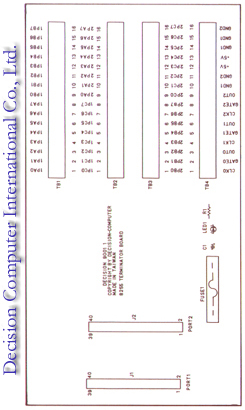
1. TB1
| PORT 1 | PA0 |
| PORT 1 | PA1 |
| PORT 1 | PA2 |
| PORT 1 | PA3 |
| PORT 1 | PA4 |
| PORT 1 | PA5 |
| PORT 1 | PA6 |
| PORT 1 | PA7 |
| PORT 1 | PB0 |
| PORT 1 | PB1 |
| PORT 1 | PB2 |
| PORT 1 | PB3 |
| PORT 1 | PB4 |
| PORT 1 | PB5 |
| PORT 1 | PB7 |
| PORT 1 | PC0 |
| PORT 1 | PC1 |
| PORT 1 | PC2 |
| PORT 1 | PC3 |
| PORT 1 | PC4 |
| PORT 1 | PC5 |
| PORT 1 | PC6 |
| PORT 1 | PC7 |
| PORT 2 | PA0 |
| PORT 2 | PA1 |
| PORT 2 | PA2 |
| PORT 2 | PA3 |
| PORT 2 | PA4 |
| PORT 2 | PA5 |
| PORT 2 | PA7 |
3. TB3
| PORT 2 | PB0 |
| PORT 2 | PB1 |
| PORT 2 | PB2 |
| PORT 2 | PB3 |
| PORT 2 | PB4 |
| PORT 2 | PB5 |
| PORT 2 | PB6 |
| PORT 2 | PB7 |
| PORT 2 | PC0 |
| PORT 2 | PC1 |
| PORT 2 | PC2 |
| PORT 2 | PC3 |
| PORT 2 | PC4 |
| PORT 2 | PC5 |
| PORT 2 | PC6 |
| PORT 2 | PC7 |
4. TB4
|
CLK0
|
|
GATE0
|
|
OUT0
|
|
CLK1
|
|
GATE1
|
|
OUT1
|
|
CLK2
|
|
GATE2
|
|
OUT2
|
|
GND1
|
|
GND2
|
|
+5V
|
|
-5V
|
|
GND1
|
|
GND1
|
|
GND2
|
