
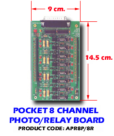
INTRODUCTION
The 8 channels relay output / photo isolator input board for pocket DIO provides relay output functions and photo isolator input functions. The relay output part provides 8 Single Pole Single Throw (SPST) relays to drive 8 different output channels. Each relay channel can be used to control ON / OFF of external devices, to drive external high power relays, to activate alarms ...etc.
The photo isolator
input part provides 8 photo couple digital input channels, which allow
the input signals to be completely floated and prevent the ground loop.
The features of 8 channels relay output / 8 channels photo isolator input board are:
*Support 8 relay
output channels and 8 photo couple input channels.
*Max contact rating for relay: 120V AC/DC 1AMP.
*Attraction time for relay: 3 ms.
*Fall off time for relay: 2 ms.
*Isolation resistance for relay: 100M OHM.
*Life expectancy for
relay: 5 million operation at full load.
*The Normal Open (NO) and Common contacts (COM) of each relay is
brought out to the screw connector.
*Breakdown voltage : AC/DC 500V minimum.
*Allow the photo input signals to be completely floated and prevent the
ground loops.
*Input current : 80mA maximum for each isolated input.
*Input voltage : 15V DC maximum for each isolated input.
*LED indicates when corresponds channel is activated.
*Isolated or non-isolated modes selectable.
*Operating temperature 0 to 60 oC.
*Storage temperature ¡V20 to 70 degree oC.
*Humidity 5% to 95%
in non-condensing
1. Terminal Board
The figure of pocket
DIO terminal board is shown on the following page.
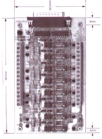
Before you use the terminal board, you must be sure to have this board plugged into pocket DIO.
The LED17 in terminal board shows the power on status. When it turns to light, we have power to this board, otherwise when it does not light, no power is provided.
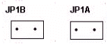
The Jumpers are used
to select isolated or non-isolated mode, when open the jumpers, it sets
to isolated mode, otherwise when short the jumpers, it sets to
non-isolated mode. JP1 and JP2 correspond to channel 0, JP3 and JP4
correspond to channel 1, etc. When set to non-isolated mode, the IxL is
short to system ground. (where x is the channel number)
2.2 Pin Assignment of TB1 (Photo Isolator)
| Pin | Description |
| 1 | I0H |
| 2 | I0L |
| 3 | I1H |
| 4 | I1L |
| 5 | I2H |
| 6 | I2L |
| 7 | I3H |
| 8 | I3L |
| 9 | I4H |
| 10 | I4L |
| 11 | I5H |
| 12 | I5L |
| 13 | I6H |
| 14 | I6L |
| 15 | I7H |
| 16 | I7L |
| Pin | Description | Pin | Description |
| 1 | GND | 14 | +5V |
| 2 | DI0 | 15 | GND |
| 3 | DI1 | 16 | GND |
| 4 | DI2 | 17 | GND |
| 5 | DI3 | 18 | GND |
| 6 | DI4 | 19 | GND |
| 7 | DI5 | 20 | DO3 |
| 8 | DI6 | 21 | DO4 |
| 9 | DI7 | 22 | DO5 |
| 10 | DO0 | 23 | DO6 |
| 11 | DO1 | 24 | DO7 |
| 12 | DO2 | 25 | +5V |
| 13 | GND |
| Pin | Description |
| 1 | COM0 |
| 2 | OTO0 |
| 3 | COM1 |
| 4 | OTO1 |
| 5 | COM2 |
| 6 | OTO2 |
| 7 | COM3 |
| 8 | OTO3 |
| 9 | COM4 |
| 10 | OTO4 |
| 11 | COM5 |
| 12 | OTO5 |
| 13 | COM6 |
| 14 | OTO6 |
| 15 | COM7 |
| 16 | OTO7 |
