
INTRODUCTION
The pocket A/D terminal board provides the standard voltage divider circuit for pocket A/D only, it supports 11 channels terminal loop, and user can design voltage divider circuit by himself.
The maximum input voltage for each channel is 0 to 5V DC or 0 to 10V DC.0
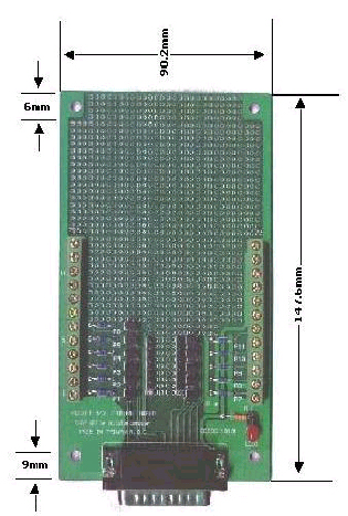
1. Terminal Board
The figure of pocket
A/D terminal board is shown on the following page
 |
Before you use the A/D terminal board, you must be sure to have this board plugged into the pocket A/D.
The LED in terminal
board shows the power on status. When it turns to light, we have power
to this board, otherwise when it does not light, no power is provided.
2.2 Pin Assignment of TB1 (Photo Isolator)
| Pin | Description | Pin | Description |
| 1 | GND | 14 | NON |
| 2 | CH0 | 15 | GND |
| 3 | CH1 | 16 | GND |
| 4 | CH2 | 17 | GND |
| 5 | CH3 | 18 | GND |
| 6 | CH4 | 19 | GND |
| 7 | CH5 | 20 | GND |
| 8 | CH6 | 21 | GND |
| 9 | CH7 | 22 | GND |
| 10 | CH8 | 23 | GND |
| 11 | CH9 | 24 | GND |
| 12 | CH10 | 25 | +5V |
| 13 | GND |
| Pin | Description |
| 1 | CH0 |
| 2 | GND |
| 3 | CH1 |
| 4 | GND |
| 5 | CH2 |
| 6 | GND |
| 7 | CH3 |
| 8 | GND |
| 9 | CH4 |
| 10 | GND |
| 11 | CH5 |
| 12 | GND |
| Pin | Description |
| 1 | CH6 |
| 2 | GND |
| 3 | CH7 |
| 4 | GND |
| 5 | CH8 |
| 6 | GND |
| 7 | CH9 |
| 8 | GND |
| 9 | CH10 |
| 10 | GND |
 |
